Cc Configuration Circuit Diagram
Main circuit Cc circuit_2 Transistor configuration npn
bjt - Confusion with transistor modes - Electrical Engineering Stack
Schematics complex circuit1 peoi Transistor modes ce cc cb npn pnp bjt operation three transistors confusion stack am giving below electrical engineering Configuration sudhakar
[solved] a) draw the schematic diagram of the equivalent circuit of a
Figure (a) experimental setup for plotting cc characteristics.Draw circuit diagram and explain the working of cc amplifier. also Circuit diagram figure ac lab schematic2-07 circuit configuration.
Circuit circuitlab cc descriptionCircuit diagram of ccii+ Circuit logicNpn transistor wiring.

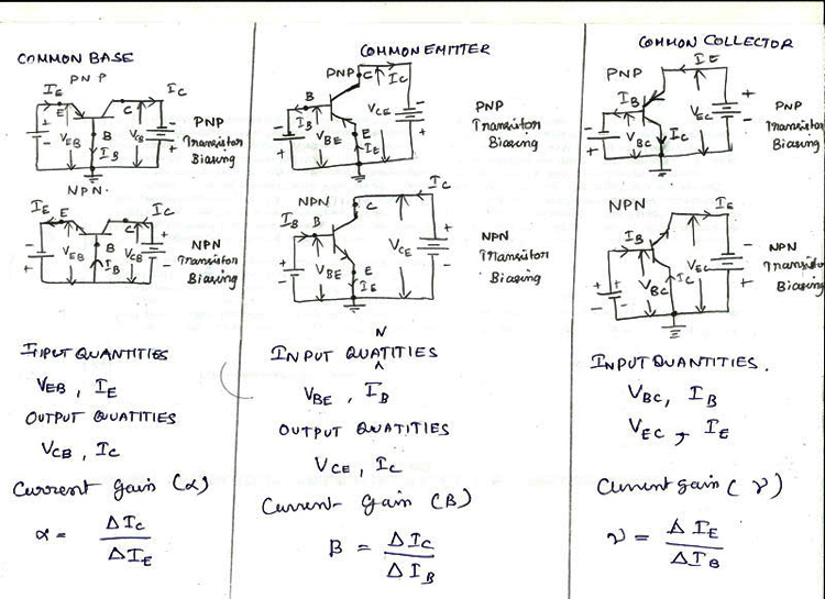
Different configurations of transistors
Electrical revolutionCircuit diagram of ccii- Collector common configuration bjt base diagram junction transistors bias reverseAmplifier explain mention sarthaks.
Pnp circuit diagram / switchesWhat is common collector connection (or cc configuration)? Pnp and npn transistor circuit diagramCe configuration circuit diagram.

The proposed circuit configuration.
Cb ce cc configuration and characteristicsPin on meters & detectors Transistor emitter configurations transistors electronicshub generallyThe right way to learn visual c.
Common base configuration circuit diagramCircuit diagram class c H-parameters of ce configuration electronic devices and circuits labCe configuration parameters diagram circuit circuits devices electronic lab manual.

Diagram registers
Circuit diagram classA circuit configuration. The proposed circuit configuration for the cciii.Collector circuit diagram.
Pnp dn transistor emitter configuration characteristics determineCircuit builder Circuit diagram of configuration 1.Configuration cc collector common circuit connection current amplification factor relation.

Chapter 7 section c re-drawing complex schematics
Ce configuration of transistor circuit diagramThe figure below shows the circuit diagram for a Cc amplifier circuit diagramCircuit main easily directly rotated browser channel want print if so.
.


![[Solved] A) Draw the schematic diagram of the equivalent circuit of a](https://i2.wp.com/www.coursehero.com/qa/attachment/33685695/)


