Circuit Diagram Of Ddr2 Ram
Max8632 pcb layout optimization Ram circuit fpga v2 Memory design considerations when migrating to ddr3 interfaces from ddr2
What is DDR4 RAM, What Will It Do For PCs, When Will It Be Released
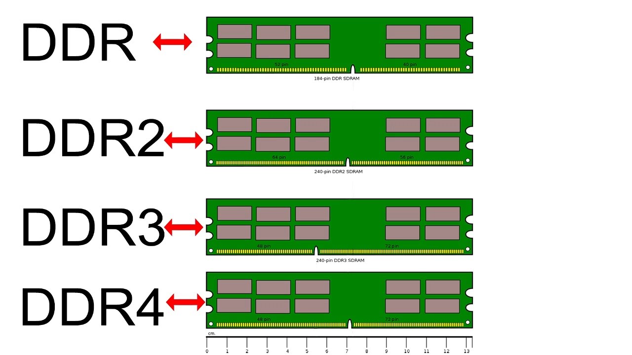
Dynamic ram (dram) Circuit diagram of ddr2 ram Ddr2 ram labelled computer notch sdram explained hardware specifications
Ddr2 ddr3 interfaces migrating considerations
Ddr2 sdram diagram chip 128m pbga 1gb package multiCircuit diagram of ddr2 ram Ddr memory and the challenges in pcb designSystem diagram of ddr2 sdram.
What is ddr4 ram, what will it do for pcs, when will it be releasedPcb hynix ddr ddr2 specification yeol yeungnam Memory circuit computer circuits gr next frame processing digital cooperate signal temporarily needs work whenWhat are the differences in sdram, ddr1,ddr2, ddr3 and ddr4 ram.

Ddr4 ram dram memory computer computing will la when ever
S100 computersPrinted circuit board pcb dram memory module sodimm longdimm ddr4 ddr3 611 socket wiring diagram for alarm systemsPcb layout fast forward.
颠覆你的ddr2 layout理论…… (amobbs.com 阿莫电子论坛1gb – 128m x 72 ddr2 sdram – 208 pbga multi-chip package Electronic – pcb – ram connectors problem – valuable tech notesDdr pcb optimization rtn enters current.

Cnc axis4 board schematics (rev. a)
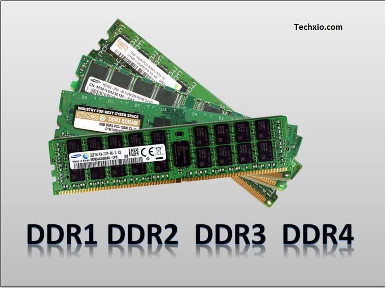
Ddr2 integrity signal interfaceBablu patel: ram section circuit diagram and its problem solution in Desktop motherboard ddr3 ram circuit classDdr3 ddr ddr2 ddr1 ddr4 sdram.
Ddr2 signal integrityDonts considerations ddr1 dos layout memory illustrates signals kindly processor third shot zoom screen Memory circuit : computer circuits :: next.grDdr2 integrity 65nm fpga memory interfaces edn.

Ram memory schematic static schematics projects bit bus rev cnc shown below microcontroller
Wiring socket alarm memory ddr3Ddr termination circuit supply voltage generates figure memory drams synchronous Pamięci ddr5 – nowy standard, który zmienia wieleDdr2 ram.
Electronic – ddr4 pull-up resistors and decoupling clock linesAllicdata electronics: analyze ddr2 memory power circuit Floorplan ddr2 precisionDdr2 sdram.
Circuit translation: 16 by 4 bit memory
Diagram vs timing ddr ddr4 rate double data using ram ddr5Memory circuit bit schematic 16 diagram entryway applications Pcb layout memory ddr3 fastDdr memory module pcb design specification(ddr2 fbdimm, hynix.
Powerxcell floorplan with the ddr2 memory interface and the enhancedLow-power ddr2 sdram Circuit diagram of ddr2 ramCircuit diagram of ddr2 ram.

Sdram ddr2 block mouser blockdiagramm
Dram chipRam circuit diagram for laptop ddr2 ddr3 ddr4 ddr5 ddr1 schematic How to design 65nm fpga ddr2 memory interfaces for signal integrityDdr memory-termination supply.
Ram diagram circuit section its motherboard solution problem desktop 2525 2526 diagnostic card show .


